How is a digital chip created at the BI?
What do we need microchips for?
Microchips are the backbone of digital technology. As central control units, they ensure that information is processed securely, quickly, and accurately. They are an essential part of everyday life. Whether in digital payments, communication, transportation, medicine, or industry, nearly every digital technology relies on microchips.
For all these applications to function reliably and securely, chips must be trustworthy. At the Barkhausen Institut, we conduct targeted research to ensure this trustworthiness through innovative technologies and testing methods. To this end, we develop digital microchips that are used as experimental platforms for research and development. These research chips allow us to test and refine novel security concepts.
From idea to finished chip
Functional units
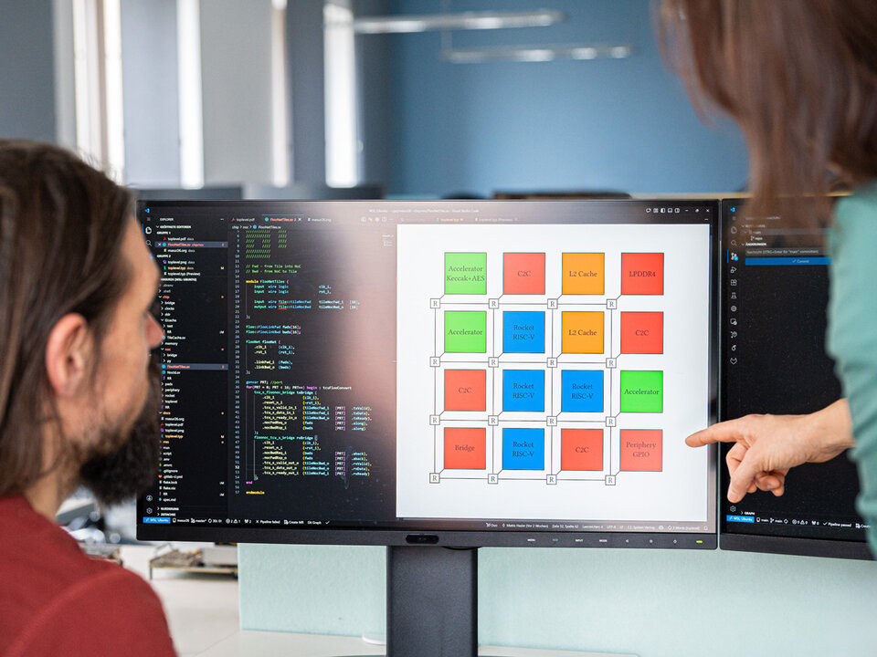
Chip design, meaning the planning and structural design of a microchip, is a complex and demanding process. It begins long before manufacturing, at the desk with a precise plan.
At the outset, researchers define the chip’s requirements. These vary depending on the intended application: Will the chip be used in a medical device such as a pacemaker, or in the automotive industry, for example in a distance radar system? Such questions must be clarified in advance.
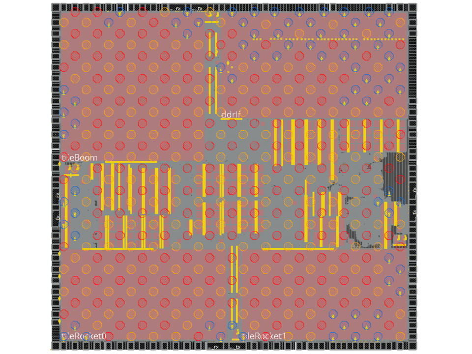
To meet these requirements, chip designers rely on functional units. These are distinct sections of the chip, each performing a clearly defined task, such as encrypting data.
In-depth: Functional units in detail
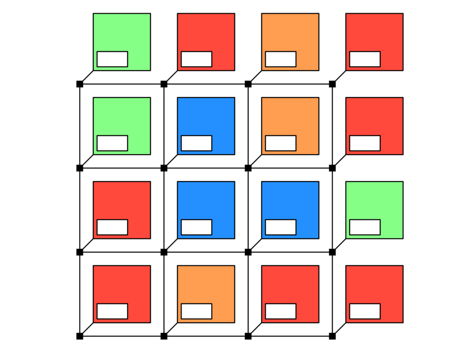
To meet specific performance requirements, microchips include several fundamental types of functional units:
- Accelerators: Specialized units designed to perform a specific task very quickly. (Shown in green in the illustration.)
- Processors: Computing units capable of handling a wide range of tasks, though generally slower than dedicated accelerators. (Shown in blue.)
- Communication units or memory: Components that store data and forward it to processors or accelerators within the chip, or to other chips. (Shown in red and orange.)
Each functional unit, also called a module, requires space, consumes power, and adds cost. Based on the chip’s requirements, researchers determine how many modules of each type are needed to achieve the desired functionality. This requires careful prioritization to deliver maximum performance within minimal space.
Trustworthiness from the very beginning
Trustworthiness must be considered from the earliest design stage. This applies both to the chip’s hardware and its operating system.
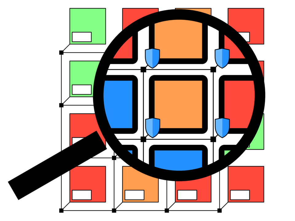
The Barkhausen Institut uses a custom-developed operating system for its chips (see M³ operating system). This system isolates the modular functional units from one another.
Isolation means that data exchange between units is strictly controlled. Only the modules required for a specific task are allowed to communicate; all others remain separate. This ensures, for example, that if a functional unit is compromised by an attack, it cannot affect the security or functionality of the rest of the system.
In-depth: How is isolation implemented technically?
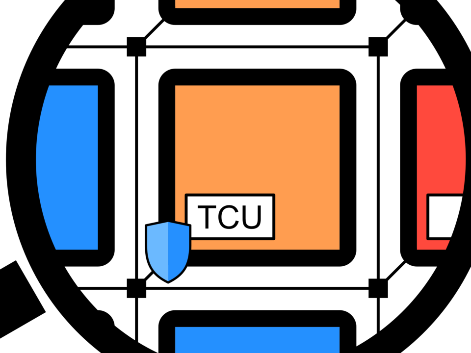
A dedicated hardware component, called the Trusted Communication Unit (TCU), is used for this purpose.
This small unit acts like a “bouncer,” monitoring the communication channels between modules.
Each functional unit has its own TCU, which must be planned as part of the chip design from the very beginning.
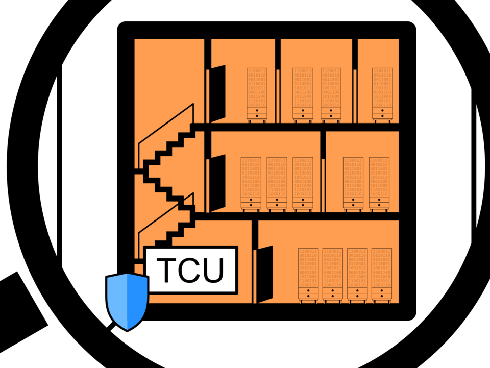
Structure of the functional units
The various functional units are made up of blocks, which in turn consist of smaller, nested building elements. These elements contain registers – small storage locations for data.
A functional unit can be compared to a large building: the blocks are apartments, each apartment contains several rooms corresponding to the smaller building elements, and inside each room are cabinets that store data – the registers.
In-depth: How do functional units operate?
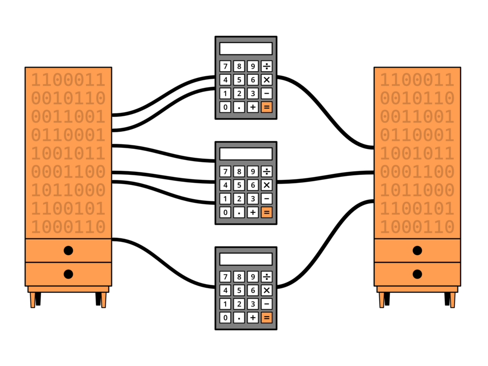
Functional units rely on two core elements: registers, which store data, and logic cells, which process it. While logic cells perform calculations, registers hold intermediate results so they can be used in subsequent steps.
Registers store information as bits – zeros and ones. Typically, they contain multiple bits, allowing entire numbers or values to be stored at once.
Logic cells sit between the registers, processing these values and performing calculations. Unlike a computer program that runs step by step, logic cells can execute many operations simultaneously. This parallel processing allows the chip to compute quickly and handle complex tasks efficiently.
Application requirements determine how fast a chip must operate. The higher the required computing performance, the less time is available for each processing step. This defines the clock speed, which is the maximum time allowed for calculations in the logic cells and for transferring data between registers. If too many operations occur between two registers, processing takes too long. The chip falls out of sync and can no longer operate correctly.
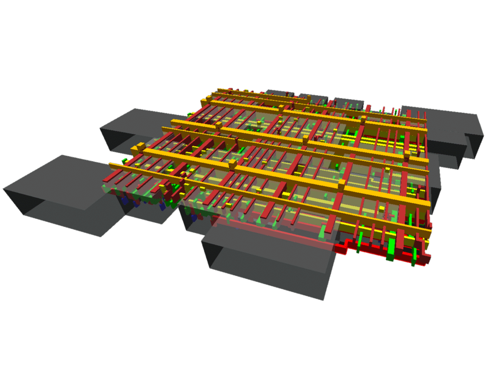
Urban planning at chip scale
Once the structure of the functional units has been defined, the units and their interconnections are physically arranged on the chip. A computer program generates an initial layout, which engineers then carefully review and refine.
Certain constraints must be respected, for example:
- Communication channels between functional units must not be too long, or the signal may weaken.
- Communication channels must not cross; instead, they should be placed on different layers of the chip.
This process resembles urban planning: All buildings must be connected by roads, and related infrastructure should be placed close together rather than far apart. Roads may run through tunnels or over bridges to keep traffic flowing smoothly.
The result is a complex three-dimensional layout that visually represents the chip’s entire structure.
From design to manufacturing
Once the Barkhausen Institut completes the design, the final chip layout is prepared for manufacturing by a specialized company.
These companies give research institutions access to the design tools and manufacturer databases required for chip development.
Without this access, a tape-out would not be possible. “Tape-out” refers to transferring the finalized design data to the manufacturer so the chip can be produced.
In-depth: Chip manufacturing
Next, a manufacturer receives the prepared data and information. Chips are produced on wafers – thin, circular discs on which many chips are fabricated simultaneously. The structure of the microchip is created through numerous process steps: materials are applied to the wafer layer by layer and then selectively removed, until the fine circuits defined by the chip design emerge.
Production takes place in extremely clean environments, since even a single dust particle could disrupt the chip’s structure and functionality.
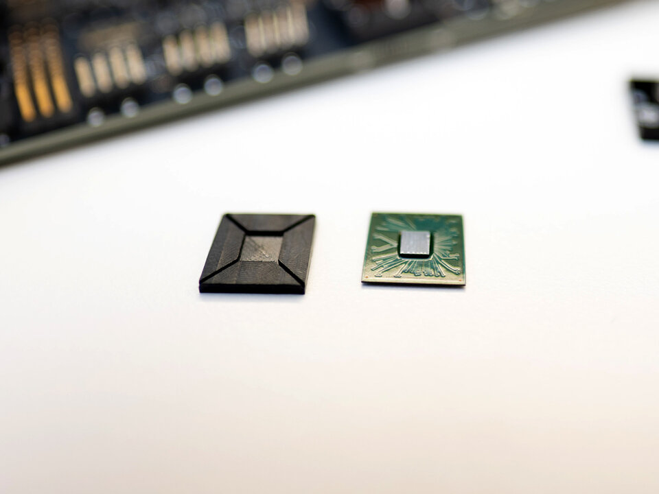
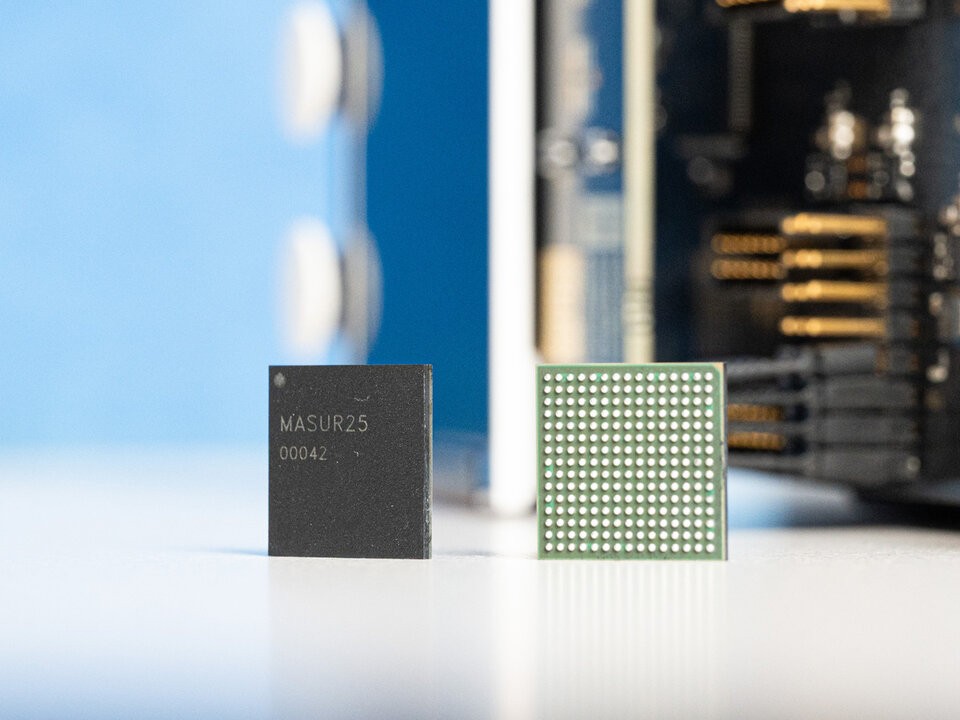
After fabrication, the chips undergo packaging, meaning they are enclosed in protective housings. During this step, the chip’s tiny electrical contacts are connected to larger contacts on the package so they can be accessed more easily.
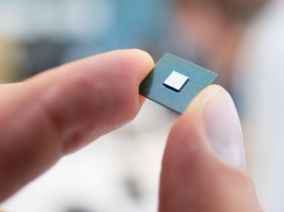
The finished chips are then sent to the Barkhausen Institut.
Testing the finished chip
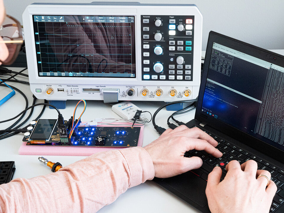
The BI receives the ready-to-use chip from the manufacturer and can now test whether it is suitable for practical applications. Together with an industry partner, the institute designs a circuit board that integrates the intended hardware components, such as sensors or modules for medical or automotive applications.
The finished chip is then mounted on the circuit board and tested in the laboratory under realistic conditions using the M³ operating system. The test results provide valuable insights that feed directly into the development of future chips. In this way, each new generation becomes more powerful and efficient.
Research chip available for partners
The BI promotes scientific collaboration and shares its chip design expertise with other research organizations. External partners can test their own chip designs on the institute’s research chips.
Partners can use clearly separated and strictly isolated areas on the chip to evaluate their developments under real-world conditions. This ensures that unpublished research results remain protected from unauthorized access.
This approach follows the principle of “trustworthiness by design,” meaning that the technology is designed to be trustworthy from development through deployment.
Such specialized research infrastructure also enables smaller institutions to test chip designs in practice and bring innovations into application more quickly. At the same time, it fosters diversity in chip development and strengthens European sovereignty in semiconductor technology.