Analog mixed-signal radio chips
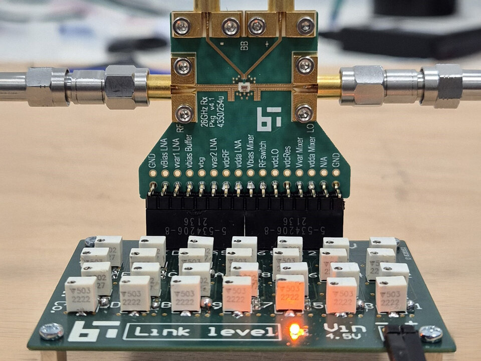
The Barkhausen Institut (BI) develops analog mixed-signal radio chips as a foundation for innovative and trustworthy hardware solutions. The RF Design Enablement group oversees the entire process - from circuit design and high-frequency-optimized antenna engineering to physical implementation (layout design) using state-of-the-art semiconductor technologies within the Silicon Saxony microelectronics cluster. Chip packaging and printed circuit board (PCB) co-design is precisely tailored to meet the demanding requirements of analog high-frequency applications.
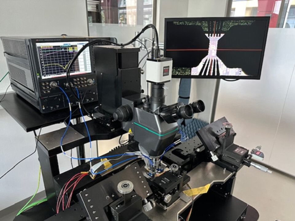
Following fabrication, comprehensive functional testing and system-level evaluations are carried out in the BI laboratories. These enable detailed analysis of signal integrity and component interoperability within the overall system in advance, reducing potential errors and improving development quality.
Analog mixed-signal radio chips developed at BI are used wherever high-precision signal processing and maximum reliability are essential - such as in safety-critical communications, advanced sensing, and industrial automation.
In addition to circuit design and fabrication, the BI’s analog chips emphasize a holistic understanding of signal processing within the overall system. State-of-the-art system simulations and parametric testing make it possible to identify and precisely optimize complex interactions in analog mixed-signal design at an early stage. This ensures the high reliability and precision of the chips - qualities that are indispensable in safety-critical applications.
Key Features of analog mixed-signal radio chips at the Barkhausen Institut:
- High-frequency-optimized mixed-signal design, including innovative antenna concepts
- Holistic system simulations for precise fault detection and targeted optimization
- Fabrication using leading-edge semiconductor technologies within the Silicon Saxony cluster
- Custom-designed chip packages and PCBs for optimal high-frequency communication
- Extensive characterization and functional testing in our in-house laboratory
- Development of chips for specialized applications such as joint communications & sensing and computed tomography
- Deployment in safety-critical communications, complex sensing, and industrial automation
- Close integration of high frequency/analog designs with digital platform chips for synergistic solutions
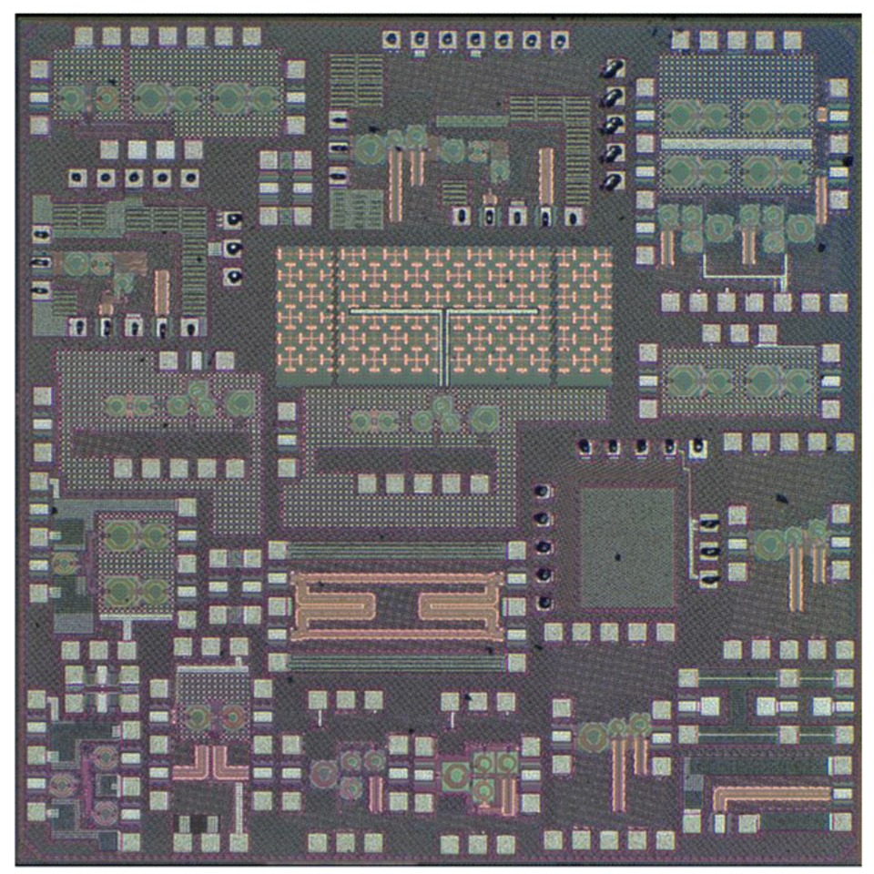
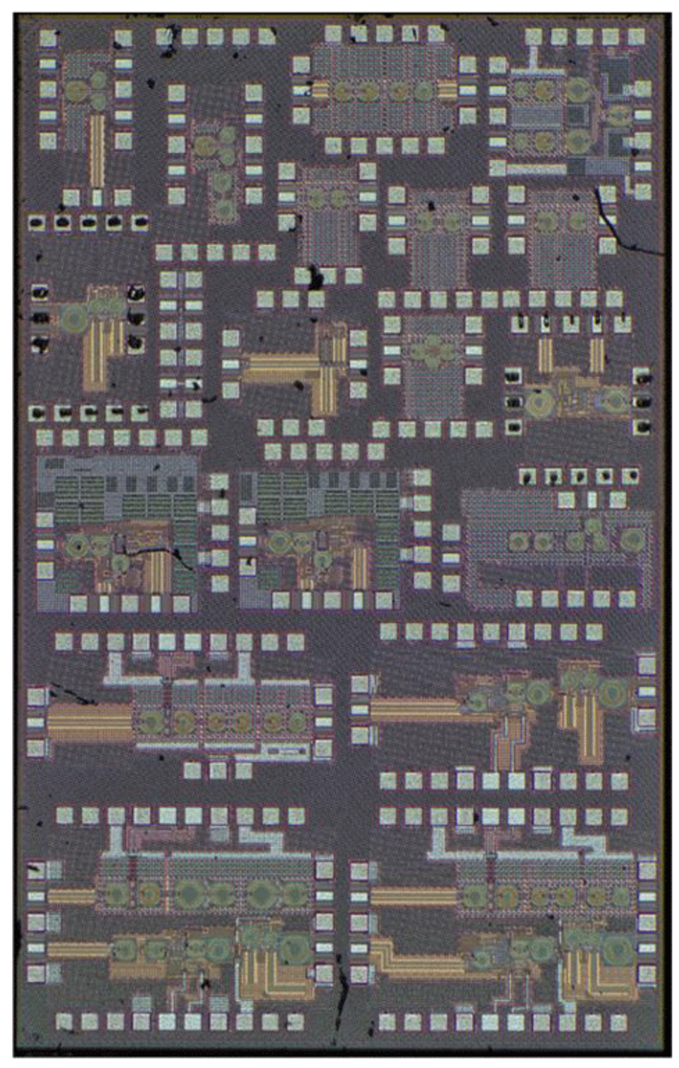
Mixed-signal radio chip Tapeouts (TPO) at the Barkhausen Institut
TPO1 (2020)
- First building blocks
- Design flow setup
- LNA, VCO, PA, transformer blocks at 26 and 60 GHz
TPO2 (2021)
- Second generation of building blocks
- On-chip de-embedding structures
- VCOs, Power detector, LNAs, passive structures at 26 and 60 GHz
TPO3 (2022)
- Reconfigurable LNA’s for 6G applications
- Active RFID Tag at 60 GHz
- On Chip antenna at 60 GHz
TPO4 (2023)
- Complete transmitter and receiver blocks at 26 GHz
- PA’s and LNA’s at 26, 60 and 77 GHz
- Electrically balanced duplexer for full duplex applications for FR2 band
TPO5 (2024)
- Building blocks for computer tomography applications
- OOK transmitter at 60 GHz
- Mixer-First Receiver at 60 GHz
TPO6 (2025)
- JTAG interface
- Full-Duplex Transceiver at 26 GHz
- IQ receiver at 26 GHz
- Mixer-First receiver at 26 GHz
TPO7 (early 2026, planned)
- Multi-band receivers
- Full Duplex Transceiver with Analog /RF self-interference cancellation (SIC) at 26 GHz
- Adaptive transmitter and receivers for FR3 bands
- IQ-Transceiver at 26 GHz
TPO8 (2026, planned)
- 3rd party DAC/ADC integration with existing RF transceiver for FR3 band
- Feasibility study on integration of full baseband solution in Masur chips
Teaching
Joint Communication and Sensing RF Hardware (EuI-NES-E-HJCAS)
This module will provide the foundation of hardware system design towards joint communication and (radar) sensing applications. The module contains details about RF front-end components and different antenna choices connecting to system development. It will also cover recent research activities in this field leading to an in-depth understanding of hardware design and measurement characterization for future applications based on key performance indicators.
Lecturer: Dr. Padmanava Sen , Course Supervisor : Prof. Dr. Gerhard Fettweis
Physical Design (English only)
Physical design is an integral part of development of digital hardware. The content taught in this course will help the students to plan and execute implementations of systems like processors, advanced VLSI systems design and physical layers of communications.